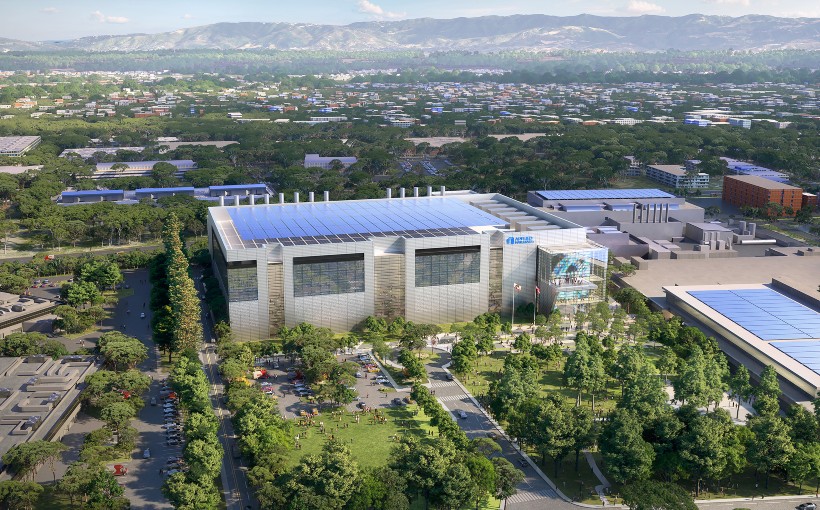
Applied Materials, Inc. announced on Monday that it will be constructing the world’s largest and most advanced facility for collaborative semiconductor process technology and manufacturing equipment research and development. The Equipment and Process Innovation & Commercialization (EPIC) Center is set to be built on an Applied Materials campus in Sunnyvale within Silicon Valley, with a projected investment of $4 billion.
The new center will encompass more than 180,000 square feet of cleanroom space for collaboration between chipmakers, universities, as well as ecosystem partners. This endeavor is expected to reduce the time it takes to bring a technology from concept to commercialization by several years.
Gary Dickerson – President & CEO of Santa Clara-based Applied Materials – commented: “This investment presents a golden opportunity to re-engineer how the global industry works together in order deliver foundational semiconductor process technologies needed for rapid improvements in energy-efficient computing performance.”